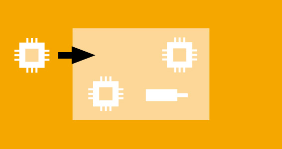
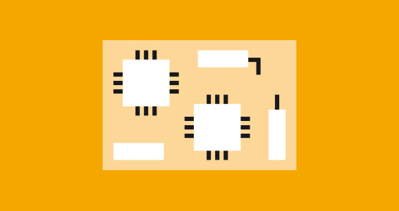
Electronics & semiconductor
Highly-complex components and higher production speeds are characteristic of today’s electronics production. Our camera technology ensures accurate measurement results with maximum performance throughout all of the steps of your production process. With our vision solutions, you can ensure that your quality assurance and process optimization standards are fit for the future.
Automatic assembly
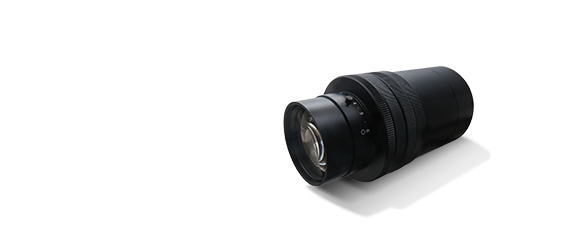
The level of quality in PCB production depends on the exact positioning of the components on the circuit board. If you want to improve the repeat accuracy in your pick and place processes we can offer you comprehensive advice and individual product solutions. We supply state-of-the-art high-precision telecentric lenses that meet your requirements. In the implementation, we use the performance data specified by you as a guide.
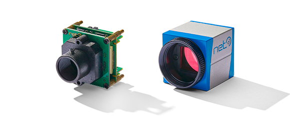
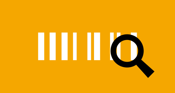
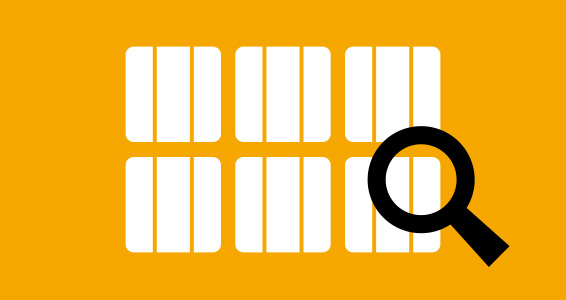
Code inspection/readers
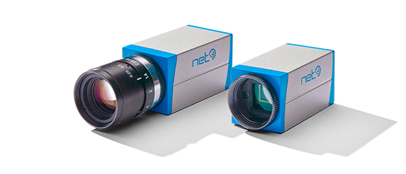
You are a semiconductor manufacturer and want to increase your throughput and level of quality? You can carry out your inspection processes in line with the latest standards with our small, powerful hardware components based on standard interfaces. The compact form of our inspection systems is ideal for the smallest areas while achieving the highest resolutions. This unlocks great potential e.g. for application in your robotic systems.
Die bonding
In production, high-resolution position measuring is standard for die bonding PCBs. Our cameras and lenses help to speed up processes and improve error tolerance. Here, we implement a high-resolution digital zoom into your camera – the “scaler”. This drastically reduces the resolution and data volume for the PC. And you can also achieve a higher frame rate with highly accurate measurements.
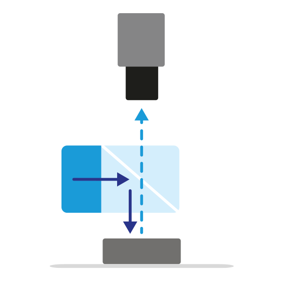
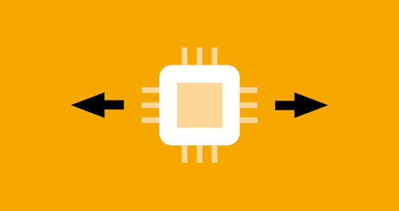
Die placement
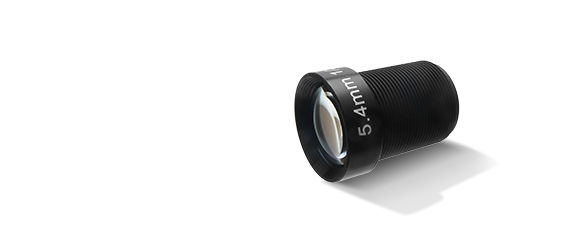
Contemporary automated die placement requires the precise detection of the contours and centers of gravity of PCBs and components. We can implement your telecentric 1:1 illustration in compliance with compact installation requirements. In this case, we offer lenses specially computed on the basis of an individual consultation. The final result is an individual vision solution that ensures both cost efficiency and high quality.
Solar wafer inspection
Our fast multi-camera systems are particularly suited to inspecting wafers for micro-cracks or faulty conductive paths. We offer several cameras for test cells which enable several wafers to be tested at the same time. A further benefit for your solar production business is our wealth of experience in the development of precisely tailored vision solutions for individual inspection tasks. We take your software and interfaces into account and guarantee fast and cost-efficient implementation.
application
is not
included?